Speakers / Lectures
Tutorial Lectures
Tutorial 1 : December 15, 14:00 – 15:00
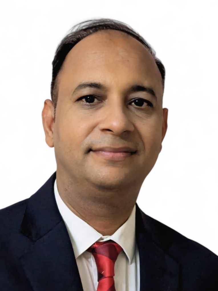
Abstract
Advance computing and high-speed wireless communications have necessitated heterogeneously- integrated packages and systems that can meet the higher throughput at lower energy. This is very different from the past of advancing each component and integrating all components necessary for a system, on system boards. Electronic packaging design is one of the most crucial aspects of the electronics industry. The new design focus, therefore, needs to be in integrated chip-package co-design.
This course focuses on four major design areas, namely signal integrity, power delivery, EMI/EMC and co-design of all these at combined chip and package levels. In that, we will learn the electrical design aspects of advanced packages and systems with a special focus on covering fundamentals of signal and power integrity, role of codesign for achieving better electrical-thermal-mechanical reliability and basics of machine learning enabled by system-level integration. An introduction to electronic packaging, signal integrity and heterogeneous integration will be discussed. We will cover the fundamental understanding of chip-to-chip signaling and design of high-speed interconnects; analysis of transmission lines and the associated SI challenges including delay, crosstalk, noise and eye diagrams. The practical aspects of power delivery and design of power distribution networks and the importance of signal and power supply noise will be covered. Finally, we will highlight the importance of chip-package co-design for improved system performance.
Tutorial 2 : December 15, 15:15 – 16:15

Abstract
This lecture presents the latest innovations in mmWave antenna-in-package (AiP) technologies
as a key enabler of high-performance wireless communication and sensing systems. It covers
advancements in high-frequency packaging substrates for compact multi-layer AiP integration,
along with signal and power integrity challenges and solutions. The lecture also includes
heterogeneous integration approaches, measurement methodologies and results, as well as an
introduction to the emerging Antennas-to-AI platform concept. This talk is supported by
MTT-S YP Outstanding Lecturer Series and MTT-S Speakers Bureau Program.
Tutorial 3 : December 15, 16:30 – 17:30


Abstract
This lecture introduces the core principles of machine learning and macromodeling, specifically tailored to the demands of high-speed interconnects and advanced electronic packaging.
It highlights data-efficient learning strategies that enable accurate, uncertainty-aware modeling for microwave and high-frequency applications.
The talk also discusses kernel-based and physics-informed system-identification methods for frequency-domain characterization of electronic components.
Together, these techniques yield interpretable, compact, and highly accurate macromodels that are ideally suited for signal- and power-integrity analysis in modern packaging technologies.
Keynote Speakers
Keynote Speech 1 : December 15, 13:00 – 13:45

Abstract
As sustaining Moore's Law becomes more challenging, advanced packaging has emerged as a critical driver of semiconductor innovation. From a back-end perspective, the ability to interconnect multiple chiplets relies heavily on interposer technology, where fine-pitch wiring and dimensional scaling play a role as fundamental as lithography does in the front-end. With the growing number of logic chips and memory stacks to be integrated, interposers are becoming larger, creating unprecedented challenges in resolution and manufacturability. At Rapidus, we are pursuing 600 mm panel-level interposer production, offering cost and throughput advantages while demanding breakthroughs in wiring miniaturization to sustain high bandwidth and low latency. This keynote highlights how packaging, once considered secondary, is now a key driver of system performance. By bridging front-end and back-end domains, we will explore innovations in interposer design, fine-line RDL lithography, and chiplet integration strategies for progress in the post-Moore era.
Keynote Speech 2 : December 16, 09:45 – 10:30

Abstract
"Moore’s law has helped us for 5+ decades through monolithic integration with packaging taking a back seat. We have now reached a stage in the semiconductor industry where advanced packaging is beginning to take the front seat, with billions of dollars being invested in it. Does this mean the end of Moore’s law? So, what has changed for packaging to take center stage? Is Heterogeneous Integration (HI) the same as what was practiced in the past? Why is AI a key driver for HI and how can HI help AI? Can HI be used to continue Moore's law?
This talk will address several of these issues in the context of emerging applications and systems. Ongoing research will be discussed during this presentation.
"
Keynote Speech 3 : December 17, 09:00 – 09:45
Abstract
High bandwidth computing applications such as graphics, games and AI have driven constant demands and innovation on packaging and interfacing. This has ranged from GDDR interfaces innovating on channel and equalization, on package memory such as the eDRAM and logic of the XBOX 360 and the current popularity and dominance of HBM for AI. What’s next? Will HBM continue to dominate innovation, or will there be a Cambrian explosion of new integrations and disintegrations of memory and computing?
Keynote Speech 4 : December 17, 09:45 – 10:30
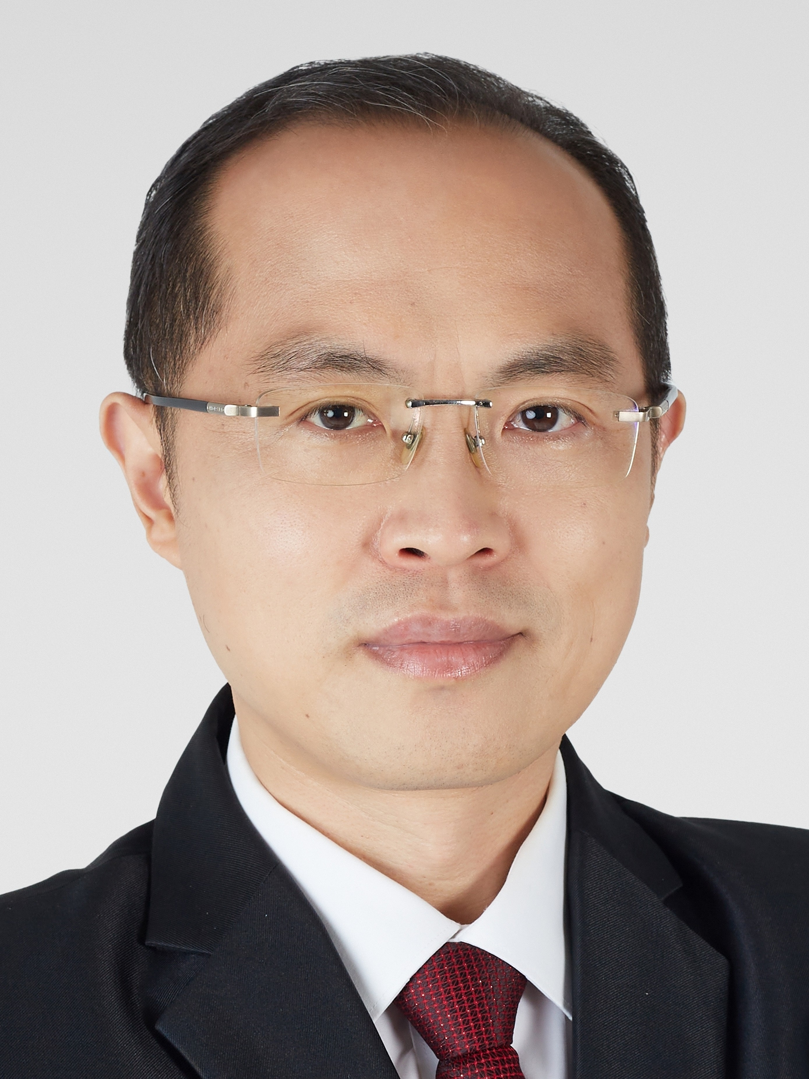
Abstract
The relentless scaling of electronic systems—from advanced IC packaging to board-level integration—has made signal and power integrity (SI/PI) challenges increasingly multidimensional, spanning wide frequency ranges, dense interconnects, and multiphysics interactions. Full-wave solvers and behavioral models, though accurate, are increasingly limited by computation time and design-space scalability. The phenomenal success of transformer-based GPT models shows the breakthrough in large-scale representation learning, which is fueling new expectations for artificial intelligence (AI) and machine learning (ML) as transformative enablers for future electronic design.
In this talk, we will first take a concise look at AI and ML, covering their historical evolution, fundamental principles, key ingredients, and representative algorithms and architectures. Building on this knowledge and understanding, we will then take a deeper look at the state-of-the art of how AI and deep learning perform in solving SI/PI problems spanning surrogate modeling, computational acceleration, optimization, and inverse and generative design.
We will conclude with a discussion of open issues, challenges, and future opportunities at the intersection of AI/ML and SI/PI for intelligent electronic design, for example, foundation models for electronic systems, where physics, data, and design automation converge in enabling the next generation of high-speed, energy-efficient electronic systems.
[Acknowledgment] the work included in this talk is partially funded by the Singapore RIE2025 MTC Programmatic Fund with the Grant No.: M23M3b0064.


